
 The G2D draws its strength upon synergy of researchers with versatile expertise in condensed matter physics, optics and photonics, soft-matter physics, solid state chemistry, ion-beam physics, and material science. This expertise and synergy provides a promise for discoveries of new phenomena in 2D materials, and potentially their applications. Particular topics to be investigated aim at (opto)mechanical, optoelectronic, spintronic, bioelectronic, capacitor, and photovoltaic applications.
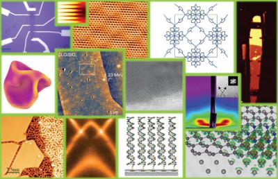
Synthesis. All large scale applications require synthesis (in large amounts) of large area 2D materials. We will explore and improve different methods of synthesis. The CVD method will be exploited under various conditions (vacuum, low pressure, atmospheric pressure) and optimised for the growth of large area (~few cm2) graphene, TMD, and h-BN single-crystal layers on metallic and other types of substrates; we will develop methods of functionalization (modify shapes, electronic properties, etc…) in electronic, optoelectronic and bioelectronic devices. We will develop transfer procedures based on novel carrier polymers and solvents which were not yet exploited, in order to obtain high-quality devices for characterization of optical and (opto)mechanical properties or to obtain high-quality electrode for solar cells. We will also develop mechanochemical methods to synthesize large amounts of 2D material, which offers greater control of the reaction course over traditional methods by establishing novel methods of high-throughput synthesis e.g. for the optimization of graphene anode in supercapacitors. Finally, we plan to produce more complex samples and by this we aim at specific properties and functionality of these complex structures. This will involve production of hybrid structures like DNA arrays on template graphene; samples and devices intercalated by magnetic or other desired proximity property materials; heterostructures obtained by combination of graphene and/or TMD and/or h-BN layers; transparent electrodes for quantum-dots based novel photovoltaic applications; defect engineered graphene and 2D materials.
Characterization. We apply a broad chain of characterization methods aiming at different physical properties. Basic sample characterization is provided through the application of Raman micro spectroscopy (Raman), scanning- and transmission-electron microscopy (SEM, TEM), scanning tunneling and atomic force microscopy (STM, AFM) characterization, and additional techniques, such as x-ray diffraction, or grazing incidence small angle x-ray scattering. In addition, more specialized experiments are envisioned to explore: optical properties of 2D materials (photodetection, photoluminescence, photoexcited carriers); macroscopic elastic properties, e.g. wrinkles and more complicated forms in porous graphite with an experimental insight obtained in newly established Laboratory for extreme mechanics; electronic transport and electronic band structure of different samples by transport methods and photoelectron spectroscopies; efficiency of 2D materials as electrodes in the photovoltaic elements; performance of graphene anode obtained from high-throughput synthesis; porosimetry for samples relevant for gas storing.
Modelling. Theoretical calculations are performed to study various electric, optical and mechanical properties of graphene and 2D materials by using the most up-to-date methods and techniques including DFT calculations (numerical), density-matrix theory calculation of the AC conductivity (perturbation theory), finite-difference time-domain Maxwell equations (numerical calculation of the optical properties of graphene based devices), and theory of elasticity (mechanical properties). In addition, for more complex structures e.g. transistors, electrodes such as gates will be implemented in vdW-DF methodology to model or predict properties of rechargeable batteries, solar cell materials, thermoelectrics and so on.