Nano-rippled graphene is a structurally modified graphene with a large range of possible applications including sensors, electrodes, optoelectronics, spintronics, and straintronics. In this work, published in the journal Carbon 96 (2016) 243, our colleagues I. Šrut Rakić and M. Kralj from Institute of Physics, together with D. Čapeta (PMF) and M. Plodinec (IRB) have shown that it is possible to synthesize macroscopic graphene sample with well-defined uniaxial periodic modulation on a vicinal metal surface and transfer it to a dielectric support without losing nano-rippled structure.

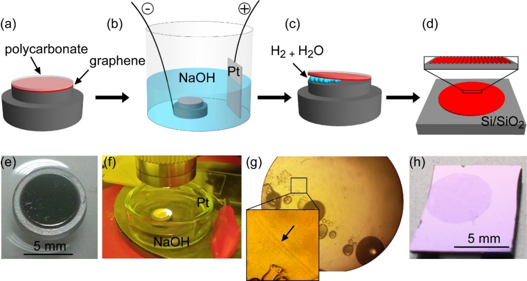
Figure 1. (a) – (d) Schematic representation of the graphene transfer procedure steps. (e) Photograph of the Ir(332) crystal covered with graphene monolayer after the sample has been taken out of UHV. (f) Photograph of an experimental setup for the bubbling transfer. (g) Optical microscopy image (x80 magnification) of the sample during the under-potential treatment. Inset shows the magnified region marked by a black rectangle where the intercalation front indicated by a black arrow can be seen. (h) Photograph of a graphene sheet after the transfer to Si/SiO2.
Structurally modified graphene recently came into focus of graphene research bringing a promise for a wider range of possible graphene applications. The key feature of such systems is a presence of curvature in graphene typically accompanied by strain. Strain has a great effect on graphene electronic structure, conductivity, optical response, and even spin transport which can then be exploited in a rippled system for fabricating targeted optoelectronic, spintronic or generally strain facilitated electronic (straintronic) devices. Moreover, properties of the rippled graphene can be useful for various sensors, electrodes, coatings and even for hydrogen storage. Therefore, it is of great importance to be able to produce a device based on rippled graphene with well-defined uniaxial, 1D, periodic modulation. The key for making such a device is the ability to synthesize and transfer structurally modified graphene to a desirable substrate of interest.

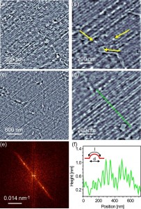
Figure 2. (a) – (d) AFM topographs at several different locations at the same sample. (e) Fourier transform image of (c) confirming the 1D ordering with a periodicity of 67 nm. (f) AFM line profile corresponding to the green line in (d). Inset shows a simplified ripple cross-section used for strain calculation.

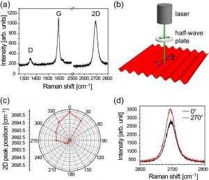
Figure 3. (a) Raman spectrum of the graphene sample on Si/SiO2 recorded with an unpolarized laser light. (b) A schematic model of the polarized laser light Raman measurement. Black arrows mark laser polarization and blue arrow marks a direction of the graphene ripples. (c) Polar plot showing positions of the 2D peak with polarized light for different laser polarization angle. (d) Raman spectra of two 2D graphene peaks for two different angles of light polarization separated by 90°.
In this paper published in Carbon (IF=6.196) the authors showed that it is possible to grow periodically nano-rippled graphene on a mm scale using a prestructured stepped Ir(332) substrate. The team carried out a transfer of such 1D modulated graphene onto a Si/SiO2 wafer adapting a method called bubbling transfer (Figure 1). The key finding upon the transfer came from AFM (atomic force microscopy) characterization showing that graphene has kept its original periodic 1D rippled structure (Figure 2). Additionally, the presence of uniaxial strain in graphene was confirmed by adapting Raman spectroscopy for polarized measurements where the laser polarization was rotated in a controlled way with respect to macroscopic ripple direction, resolving between strained and unstrained directions in graphene (Figure 3).
This work presents a collaborative interinstitutional effort within the CEMS and brings a relevant achievement for a large scale graphene applications.
