
Infrared photodetectors are a major component of many optoelectronic devices used in telecommunications, sensing, and imaging technologies. Long distance telecommunications are enabled by silica optical fibers, where near-infrared (NIR) wavelengths in the range of 1.3–1.6 μm are used due to the superior transparency of silica in this range. Heterojunctions between an organic semiconductor and silicon are an attractive route to extending the response of silicon photodiodes into the NIR range, up to 2000 nm. Silicon-based alternatives are of interest to replace expensive low band-gap materials, like InGaAs, in telecommunications and imaging applications. Micro- and nano-structuring of silicon can significantly influence its properties, which can enable enhancement of silicon-based devices by careful nano-scale optimization.
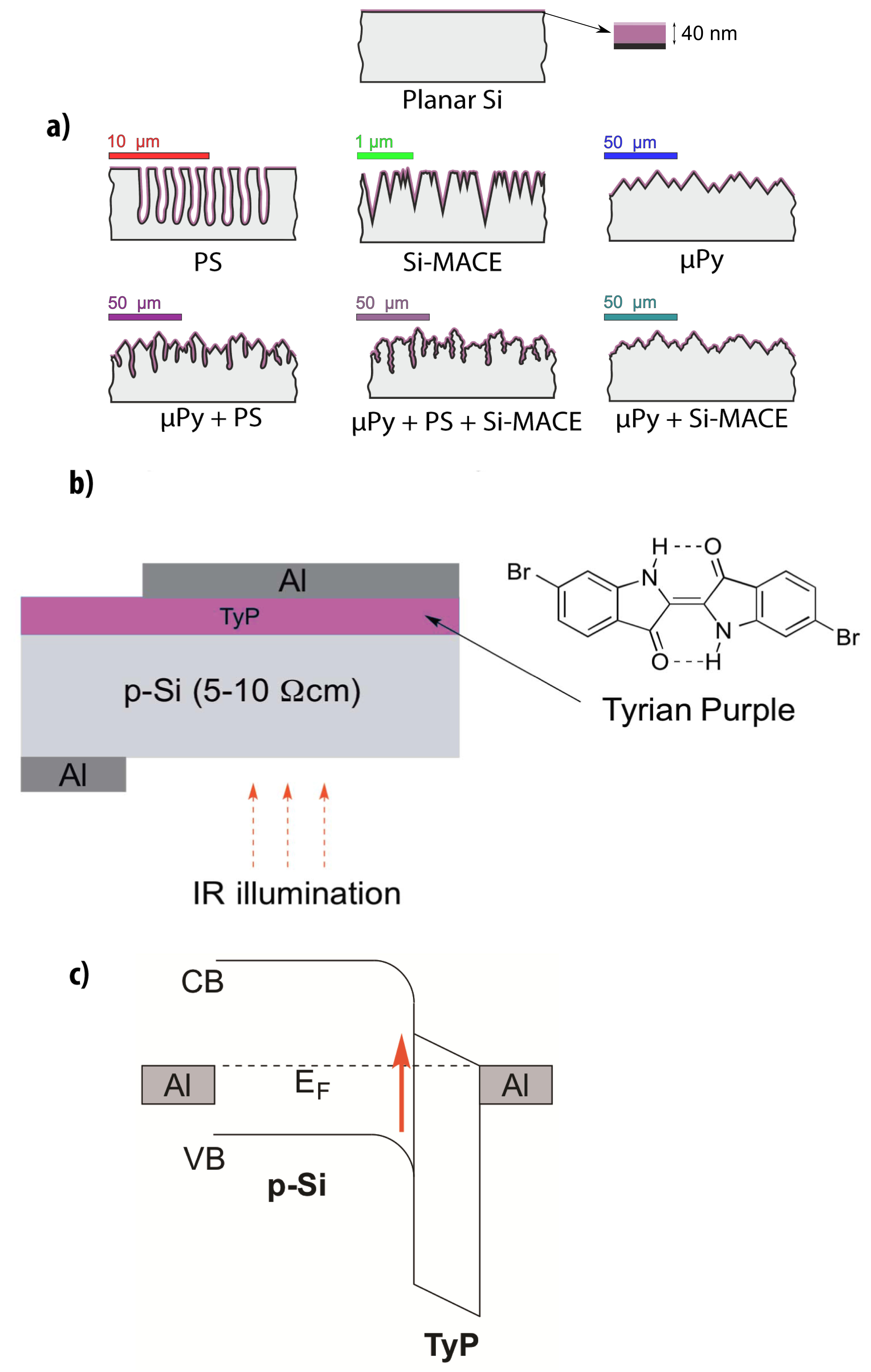
(a) Schematic representations of structured versus planar heterojunctions between silicon and a thin organic semiconductor epilayer. The upper row shows single-step structuring, while hierarchical combinations of different structuring techniques are on the second row. (b) Device schematic of an Al/p-Si/TyP/Al heterojunction device, with the molecular structure of TyP. (c) Band diagram of an Al/p-Si/TyP/Al heterojunction diode under short circuit conditions. The red arrow represents the sub-band gap NIR absorption.
The study “Enhanced near-infrared response of nano- and microstructured silicon/organic hybrid photodetectors“, published by journal Applied Physics Letters (IF 3.569) of the American Institute of Physics, is a result of collaboration of the research groups of prof. Niyazi Serdar Sariciftci, Institute for Organic Solar Cells (LIOS)/Physical Chemistry at the Johannes Kepler University in Linz, Austria and of dr. Mile Ivanda from CEMS-NFM at Ruđer Bošković Institute in Zagreb, Croatia. The research work was performed by a 5-month visit of V. Đerek to LIOS, Linz and his close collaboration with the LIOS group member Eric Daniel Głowacki. The visit of V. Đerek was supported by the Ernst-Mach-Stipendien granted by the OeAD—Austrian Agency for International Cooperation in Education & Research, financed by BMWF.
The paper reports on the significant enhancement in NIR photodetector performance afforded by nano- and microstructuring of p-doped silicon (p-Si) prior to deposition of a layer of the organic semiconductor Tyrian Purple (TyP). Heterojunction diodes with the general device structure as shown in Figure (b) were prepared with various nano- and microstructuring methods as shown in Figure (a), with planar devices always being prepared in parallel to provide an “internal” standard for a given set of measurements. A number of well-established techniques was employed to increase the interfacial area of the p-Si/organic junction, both alone and in hierarchical combinations: (1) micropyramids (μ-pyramids) with dimensions ∼10 μm; (2) metal-assisted chemically etched (MACE) porous silicon with ∼50–200 nm pores; and (3) electrochemically anodized porous silicon, with pore sizes of 10–1000 nm. It was shown how different silicon structuring techniques, namely, electrochemically grown porous Si, metal-assisted chemical etching, and finally micropyramids produced by anisotropic chemical etching (Si μP), are effective in increasing the NIR responsivity of p-Si/TyPheterojunction diodes.
In all cases, the structured interfaces were found to give photodiodes with superior characteristics as compared with planar interface devices, providing up to 100-fold improvement in short-circuit photocurrent, corresponding with responsivity values of 1–5 mA/W in the range of 1.3–1.6 μm. The measurements have shown that this increased performance is neither correlated to optical effects, i.e., light trapping, nor simply to geometric surface area increase by micro- and nanostructuring. The performance enhancement afforded by the structured p-Si/organic diodes is likely caused by a yet unresolved mechanism, possibly related to electric field enhancement near the sharp tips of the structured substrate. The observed responsivity of these devices places them closer to parity with other, well-established, Si-based NIR detection technologies.
The collaboration included a group members from CEMS-NFM, IRB, Zagreb (V. Đerek, M. Marcijuš, M. Ristić and M. Ivanda), from LIOS, Linz (E. D. Głowacki and N. S. Sariciftci) and from Friedrich-Alexander Universität, Energie Campus, Erlangen/Nürnberg (M. Sytnyk and W. Heiss).

SEM images of different nano- and microstructured Si surfaces with a 40-nm TyP epilayer evaporated on top. (a) Porous Si, (b) Si MACE, (c) Si μ-Pyramids, (d) hierarchical Si μ-pyramids/porous Si, (e) hierarchical Si μ-pyramids/MACE, and (f) hierarchical Si μ-pyramids/MACE/porous Si