Manipulation of macroscopic nano-patterned graphene

Nano-rippled graphene is a structurally modified graphene with a large range of possible applications including sensors, electrodes, optoelectronics, spintronics, and straintronics. In this work, published in the journal Carbon 96 (2016) 243, our colleagues I. Šrut Rakić and M. Kralj from Institute of Physics, together with D. Čapeta (PMF) and M. Plodinec (IRB) have shown that it is possible to synthesize macroscopic graphene sample with well-defined uniaxial periodic modulation on a vicinal metal surface and transfer it to a dielectric support without losing nano-rippled structure.

Transfer schematics

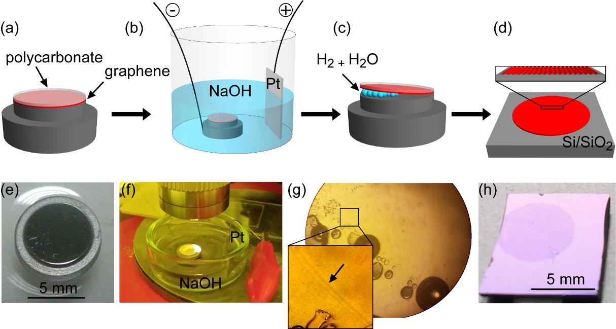
Figure 1. (a) – (d) Schematic representation of the graphene transfer procedure steps. (e) Photograph of the Ir(332) crystal covered with graphene monolayer after the sample has been taken out of UHV. (f) Photograph of an experimental setup for the bubbling transfer. (g) Optical microscopy image (x80 magnification) of the sample during the under-potential treatment. Inset shows the magnified region marked by a black rectangle where the intercalation front indicated by a black arrow can be seen. (h) Photograph of a graphene sheet after the transfer to Si/SiO2.

Structurally modified graphene recently came into focus of graphene research bringing a promise for a wider range of possible graphene applications. The key feature of such systems is a presence of curvature in graphene typically accompanied by strain. Strain has a great effect on graphene electronic structure, conductivity, optical response, and even spin transport which can then be exploited in a rippled system for fabricating targeted optoelectronic, spintronic or generally strain facilitated electronic (straintronic) devices. Moreover, properties of the rippled graphene can be useful for various sensors, electrodes, coatings and even for hydrogen storage. Therefore, it is of great importance to be able to produce a device based on rippled graphene with well-defined uniaxial, 1D, periodic modulation. The key for making such a device is the ability to synthesize and transfer structurally modified graphene to a desirable substrate of interest.

SPM karakterizacija

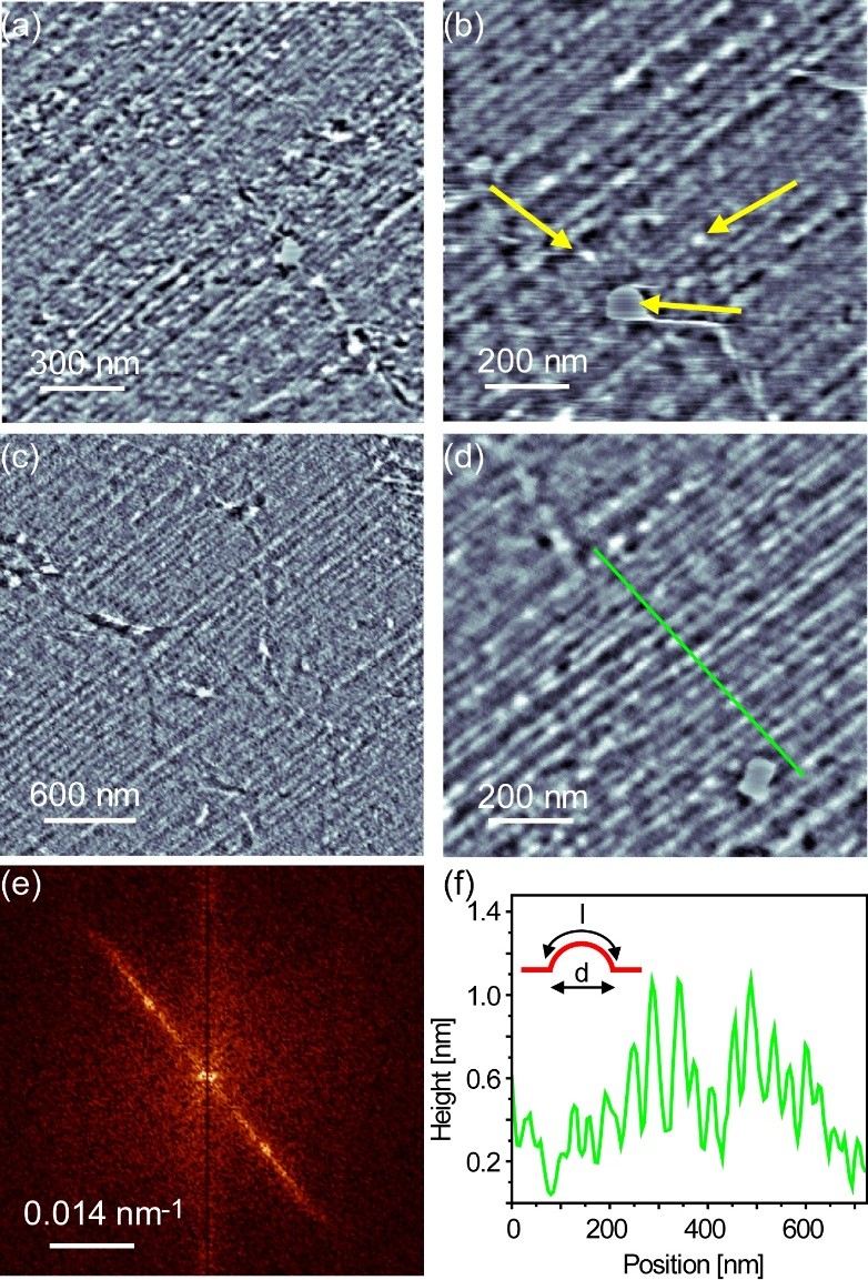
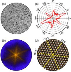
Figure 2. (a) – (d) AFM topographs at several different locations at the same sample. (e) Fourier transform image of (c) confirming the 1D ordering with a periodicity of 67 nm. (f) AFM line profile corresponding to the green line in (d). Inset shows a simplified ripple cross-section used for strain calculation.

Raman characterization

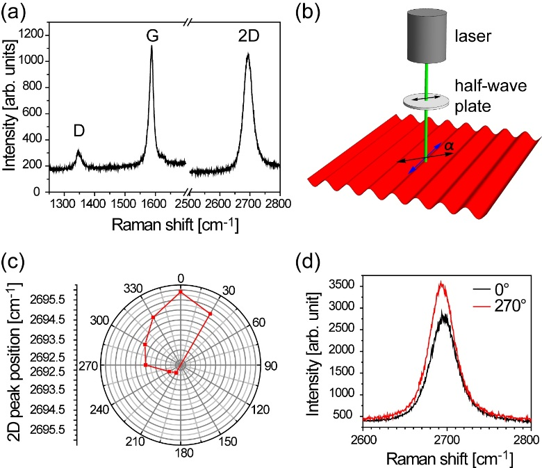
Figure 3. (a) Raman spectrum of the graphene sample on Si/SiO2 recorded with an unpolarized laser light. (b) A schematic model of the polarized laser light Raman measurement. Black arrows mark laser polarization and blue arrow marks a direction of the graphene ripples. (c) Polar plot showing positions of the 2D peak with polarized light for different laser polarization angle. (d) Raman spectra of two 2D graphene peaks for two different angles of light polarization separated by 90°.

In this paper published in Carbon (IF=6.196) the authors showed that it is possible to grow periodically nano-rippled graphene on a mm scale using a prestructured stepped Ir(332) substrate. The team carried out a transfer of such 1D modulated graphene onto a Si/SiO2 wafer adapting a method called bubbling transfer (Figure 1). The key finding upon the transfer came from AFM (atomic force microscopy) characterization showing that graphene has kept its original periodic 1D rippled structure (Figure 2). Additionally, the presence of uniaxial strain in graphene was confirmed by adapting Raman spectroscopy for polarized measurements where the laser polarization was rotated in a controlled way with respect to macroscopic ripple direction, resolving between strained and unstrained directions in graphene (Figure 3).

This work presents a collaborative interinstitutional effort within the CEMS and brings a relevant achievement for a large scale graphene applications.

Development of the MeV SIMS with sub micron resolution

The MeV secondary ion mass spectrometry (SIMS) technique is based on a concept being developed already in 1974, when the first publications about the desorption of molecular ions using fission fragments from 252Cf source (plasma desorption mass spectrometry – PDMS) appeared. In 2008, group of prof. J. Matsuo from Kyoto University started to use MeV ions from ion beam accelerator accompanied by a time of flight (TOF) mass spectrometer. Comparison to the keV energy ions (used in conventional SIMS), showed significant suppression of fragmentation and simultaneously enhancement the secondary ion yield, which is in particular evident for higher mass molecules (100-1000 Da).
In 2012, Time of Flight Secondary Ion Mass Spectrometry (ToF-SIMS) setup was constructed and installed at the RBI microbeam beam line as a result of bilateral Croatian – Japan project “Enhanced molecular imaging by focused swift heavy ions”. In attempt to make this technique widely accepted, RBI group performed numerous tests of its applicability to biomedical problems, cultural heritage studies and materials science. Presentely, this work is supported by three international projects on MeV SIMS: ITN Marie Curie SPRITE project on MeV SIMS, UKF project “Study of modern paint materials and their stability using MeV SIMS and other analytical techniques“ and IAEA CRP project “Development of molecular concentration mapping techniques using MeV focused ion beams”.

2D distribution of Na, K, and lipids in CaCo-2 cell. A STIM image (density distribution) is also presented, together with an optical image and TOF-SIMS spectrum.

2D distribution of Na, K, and lipids in CaCo-2 cell. A STIM image (density distribution) is also presented, together with an optical image and TOF-SIMS spectrum.

In the case of biomedical applications it is important to perform molecular mapping at the subcellular level. However, the beam spot size of the existing MeV TOF-SIMS systems, which is typically several microns, is too large and has to be reduced. In order to improve the lateral resolution of the focussed beam, the trigger for the TOF – START was replaced with a timing signal provided by a silicon charged particle detector used for Scanning Transmission Ion Microscopy (STIM). By using a trigger signal from detector instead of the bunching the ion microbeam, significant reduction of the object and collimator slit openings was enabled, leading to the reduction of the ion beam spot size (down to 300 nm). Altogether, due to the well-defined submicron beam focus and the high sensitivity, molecular imaging of a single cell at a sub-cellular level has been for the first time achieved by MeV TOF-SIMS as well. Results of this work has been recently published in Applied Physics Letters: Z. Siketić, I. Bogdanović Radović, M. Jakšić, M. Popović Hadžija, M. Hadžija, Submicron mass spectrometry imaging of single cells by combined use of mega electron volt time-of-flight secondary ion mass spectrometry and scanning transmission ion microscopy. In addition, the leading author of the APL paper Zdravko Siketić, presented this work by invited talk at the 13th International Symposium on Radiation Physics held in September in Beijing, China.

Response of the graphene and gallium nitride to swift heavy ion irradiation

Irradiation of flat solid surface by swift heavy ions can result in the formation of nanoscale surface features like hillocks or craters. These remnants of ion impacts called ion tracks can be observed directly using atomic force microscopy (AFM). Within the research unit Ion Beam Physics and Technology, we have demonstrated in two recently published papers that swift heavy ion beams are versatile tool for nanostructuring graphene and GaN.

Monolayer graphene after exposure to grazing incidence swift heavy ion irradiation (a) 84 MeV Ta, (b) 23 MeV I, (c) 15 MeV Si

Monolayer graphene after exposure to grazing incidence swift heavy ion irradiation (a) 84 MeV Ta, (b) 23 MeV I, (c) 15 MeV Si

In the work “Nanostructuring graphene by dense electronic excitation”, published in Nanotechnology (journal IF = 3.821) we reported detailed investigation of graphene response to the swift heavy ion irradiation in a wide range of energies. It was demonstrated that medium scale accelerator facilities like the one at the RBI can be used successfully for nanostructuring graphene (Figure 1.). By choosing appropriate ion beam irradiation parameters, not only graphene can be pierced, thus producing nanoscale pores within it, but also different kind of defects can be introduced into it in a controlled manner. The study was done in a collaboration with scientists from Germany (Universities Duisburg-Essen, Ulm and Jena), France (GANIL ion accelerator facility in Caen) and RBI (M. Karlušić, M. Jakšić).

In the work “Response of the GaN to energetic ion irradiation: conditions for ion track formation” published in J. Phys. D: Appl. Phys. (journal IF = 2.721) and featured on the journal cover page, we reported results of our investigations regarding swift heavy ion irradiation of wurzite GaN surface, and showed for the first time that grazing incidence small angle X-ray scattering (GISAXS) can be utilized for analysis of such irradiated surface (Figure 2.).

Irradiated GaN surface at IRRSUD, GANIL with 92 MeV Xe, Θ = 1°, Φ = 100/μm2 (a) AFM image and GISAXS spectra taken at different azimuthal angles with respect to orientation of the surface ion tracks: 0° (b), 2° (c), 10° (d).

Irradiated GaN surface at IRRSUD, GANIL with 92 MeV Xe, Θ = 1°, Φ = 100/μm2 (a) AFM image and GISAXS spectra taken at different azimuthal angles with respect to orientation of the surface ion tracks: 0° (b), 2° (c), 10° (d).

coverIn contrast to previous works where nanohillocks were found within the surface ion track, morphology of 92 MeV Xe ion tracks consist of both nanohillocks and nanoholes. For lower energy irradiation using 23 MeV I, ion tracks consist only of nanoholes. In addition, TOF-ERDA measurements showed significant loss of nitrogen during irradiation and opens up the question of the composition of ion tracks. The study was done by the team of scientists from the RBI ion accelerator facility (M. Karlušić, M. Buljan, Z. Siketić, M. Jakšić, B. Šantić), in collaboration with colleagues from GANIL ion accelerator facility (Caen, France), HZDR (Dresden, Germany), Elettra synchrotron (Trieste, Italy) and Universities Duisburg-Essen and Ulm (Germany).

Projects

Sorry, this entry is only available in Croatian. For the sake of viewer convenience, the content is shown below in the alternative language. You may click the link to switch the active language.

Projekti

Projects

Projects

12. “Croatian Quantum Communication Infrastructure – CroQCI“, applicant CARNET, scientific leader IRB, project leader Martin Lončarić (IRB). Financed through Horizon Europe with 50% contribution from Croatian RRF fund. Contract Nr. MZO 101091513. Total budget: 9.999.334,04 eur, RBI cca. 3.600.000,00 eur. Started 1.1.2023.

11. “Development of building blocks for new European quantum communication network”, Croatian leader: M. Stipčević, Research project Croatia-Slovenia, HRZZ grant No. IPS-2020-1-2616 started 15.10.2019. Financed by HRZZ (200 kEUR) and ARRS (300 kEUR). Project’s web page: http://cold.ifs.hr/rubidium-vapor-eit-quantum-memories/

10. “Biological and bioinspired structures for multispectral surveillance”, Croatian leader: H. Skenderović, Multi-year Science for Peace NATO Project No. G5618, started 15.10.2019. Financed by NATO

9. Feasibility Study for employing the uniquely powerful ESS linear accelerator to generate an intense neutrino beam for leptonic CP violation discovery and measurement (ESSnuSB), leader for Croatia: B. Kliček. Project No.  777419 (H2020), signed: 22.11.2017., started: 01.01.2018. Financed through Horizon 2020.

8. “Support for top-level research of Centre of excellence for advanced materials and sensing devices“, leaders M. Jakšić, M. Ivanda, M. Kralj, and M. Stipčević. Funded through European structural and 5nvestment funds (ESIF), MSE grant No. KK.01.1.1.01.0001

7.  COST action CA15139 – Combining forces for a novel European facility for neutrino-antineutrino symmetry-violation discovery (EuroNuNet), Action chair: Dr Marcos Dracos (IN2P3 Strasbourg, France), Management Committee Member: Dr Budimir Kliček (Ruđer Bošković Institute, Zagreb, Croatia)

6. “Quantum entanglement for ultra-secure communications“, Leaders: Dr. Mario Stipčević, (CEMS-IRB, Zagreb, Croatia) and Prof. dr. Rupert Ursin (IQOQI, Vienna, Austria). Duration: 2016-2017 (2 years). In this project we address scientific and technological aspects of quantum entanglement which lies in the heart of the secure information exchange, quantum cryptography, random number generation as well as some vibrant scientific research topics related to quantum information and secure communications.

5. “Holography and interferometry under weak illumination” HrZZ – IP-2014-09-7515, 01.05.2015. – 30.04.2019. Leader: Nazif Demoli, Institute of Physics (IF). Associates: Hrvoje Skenderović (IF), Davorin Lovrić (IF), Jadranko Gladić (IF), Mario Rakić (IF), Mario Stipčević (RBI), Ognjen Milat (IF), Mladen Pavičić, Denis Abramović (IF), Marin Karuza (University of Rijeka). Research areas: Optical physics.

4. “TRANSHOW1 Knowledge transfer“, leader M. Lončarić.

3. COST Action MP1406 – Multiscale in modelling and validation for solar photovoltaics (MultiscaleSolar), Action Chair: Dr James Connolly (Génie électrique et électronique de Paris), Management Committee Member: Dr Martin Lončarić, (Ruđer Bošković Institute, Zagreb, Croatia)

2. “ICT COST Action IC1306 Cryptography for Secure Digital Interaction“, Leader: Prof. Claudio Orlandi (Aarhus University, Denmark), Coordinator for Croatia: Dr. Mario Stipčević, Ruđer Bošković Institute.

1. “ICT COST Action CA15220 Quantum Technologies in Space“, Leader: Prof. Angelo Bassi (University of trieste, Italy), Coordinator for Croatia: Dr. Mario Stipčević, Ruđer Bošković Institute

Projects

2015-2019 “Hybrid Silicon Nanostructures for Sensing”, Croatian Science Foundation, project no.: IP-2014-09-7046.

2014-2019 “New functional materials”, Center of excellence for new materials and sensors, Leader: M. Ivanda, Funding source: Ministry of Science and Technology of Croatia and the Structural Funds of European Union.

Projects

HRZZ: Ion Beam Induced Changes in Crystaline Materials (MIOBICC), 2014-2018, Principal investigator, Stjepko Fazinić

HRZZ: Nuclear structure and reactions – experiments towards the neutron drip line, 2014-2018, Principal investigator, Suzana Szilner

HRZZ: Nano-networks of Quantum Dots in Glasses: From Self-assembly to Energy Conversion and Hydrogen Storage, 2014-2018, Principal investigator, Maja Buljan

EU H2020 project EuroFusion, 2014-2018, Project coordinator for RBI, Tonči Tadić

EU H2020 project AIDA – Advanced European Infrastructures for Detectors at Accelerators, 2015-2019, Project coordinator for RBI, Stjepko Fazinić

EU H2020 ERA Chair project PARADESEC – Expanding Potential in Particle and Radiation Detectors, Sensors and Electronics in Croatia, 2015-2020, Project coordinator, Neven Soić

NATO SPS project E-SiCure – Engineering silicon carbide for enhanced borders and ports security, 2016-2020, Voditelj project, Ivana Capan

IAEA CRP F11020: Development of single ion irradiation techniques and probing the induced changes in SiC and diamond , 2017-2020, Principal investigator, Milko Jakšić

IAEA CRP F11019: Development of molecular concentration mapping techniques using MeV focused ion beams, 2014-2018, Principal investigator, Zdravko Siketić

COMPLETED PROJECTS:

EU FP7 project SPRITE – Supporting Postgraduate Research with Internship in industry and Training Excellence – Marie Curie Initial Training Network, 2013-2016, Project coordinator for RBI, Milko Jakšić

UKF: Study of modern paint materials and their stability using MeV SIMS and other analytical techniques (2012-2015), Principal investigator, Ivančica Bogdanović Radović

IAEA CRP CRO-17051: Radiation hardness of semiconductors and insulators studied by focused ion beam irradiation and IBIC, 2012-2105, Principal investigator, Milko Jakšić

IAEA CRP CRO-18227: Environmental protection and monitoring of cultural heritage objects and applied research on structured materials for photo-electric energy conversion, 2014-2017, Principal investigator, Stjepko Fazinić

Bilateral project with Germany (MZOS-DAAD), Technische Universitatet Berlin, Micro X-ray Emission Spectroscopy (MIXES), 2015-2016, Principal investigator, Stjepko Fazinić

Bilateral project with Slovenia, Molecular imaging of biological samples using MeV ions and keV clusters for TOF-SIMS spectrometry, Principal investigator, Zdravko Siketić

COST Training School on Raman Spectroscopy

COSTCEMS-NFM is organizing the Training School on Raman Spectroscopy for the COST action “Nanospectroscopy” MP1302. The school will take place at the Ruder Boškovic Institute in Zagreb, Croatia, on September 23-25, 2015. Selected topics are historical introduction of the Raman spectroscopy, theory of Raman spectroscopy on molecules and crystals, surface enhanced Raman spectroscopy and applications, Raman spectroscopy of  nanoparticles, Raman scattering on disordered materials, Raman spectroscopy in materials research, Time-resolved techniques with ultrashort pulses in examination of specific vibrational states of matter, application of ESR spectroscopy in probing of vibrational states of disordered materials and practical laboratory courses on Raman spectroscopy. Guest speaker for the school is Prof. Philippe Colomban, UPMC Paris, with the topic “Raman Spectroscopy of advanced materials (fibre, composites, films, ..) for aerospace and energy application”. The preliminary program can be found here. The Training School aims particularly at Early-Stage Researchers. The number of participants for laboratory courses is limited to allow for hands-on training, but the lectures are open to the general public.

UPDATE: Presentation slides, from the tutorial lectures held during the Raman School are available here for the Raman School participants.

APL paper: Enhanced NIR response of nano-silicon/organic hybrid photodetectors

Infrared photodetectors are a major component of many optoelectronic devices used in telecommunications, sensing, and imaging technologies. Long distance telecommunications are enabled by silica optical fibers, where near-infrared (NIR) wavelengths in the range of 1.3–1.6 m are used due to the superior transparency of silica in this range. Heterojunctions between an organic semiconductor and silicon are an attractive route to extending the response of silicon photodiodes into the NIR range, up to 2000 nm. Silicon-based alternatives are of interest to replace expensive low band-gap materials, like InGaAs, in telecommunications and imaging applications. Micro- and nano-structuring of silicon can significantly influence its properties, which can enable enhancement of silicon-based devices by careful nano-scale optimization.

Schematic representations of structured versus planar heterojunctions between silicon and a thin organic semiconductor epilayer

(a) Schematic representations of structured versus planar heterojunctions between silicon and a thin organic semiconductor epilayer. The upper row shows single-step structuring, while hierarchical combinations of different structuring techniques are on the second row. (b) Device schematic of an Al/p-Si/TyP/Al heterojunction device, with the molecular structure of TyP. (c) Band diagram of an Al/p-Si/TyP/Al heterojunction diode under short circuit conditions. The red arrow represents the sub-band gap NIR absorption.

The study “Enhanced near-infrared response of nano- and microstructured silicon/organic hybrid photodetectors“, published by journal Applied Physics Letters (IF 3.569) of the American Institute of Physics, is a result of collaboration of the research groups of prof. Niyazi Serdar Sariciftci, Institute for Organic Solar Cells (LIOS)/Physical Chemistry at the Johannes Kepler University in Linz, Austria and  of dr. Mile Ivanda from CEMS-NFM at Ruđer Bošković Institute in Zagreb, Croatia. The research work was performed by a 5-month visit of V. Đerek to LIOS, Linz and his close collaboration with the LIOS group member Eric Daniel Głowacki. The visit of V. Đerek was supported by the Ernst-Mach-Stipendien granted by the OeAD—Austrian Agency for International Cooperation in Education & Research, financed by BMWF.

The paper reports  on the significant enhancement in NIR photodetector performance afforded by nano- and microstructuring of p-doped silicon (p-Si) prior to deposition of a layer of the organic semiconductor Tyrian Purple (TyP). Heterojunction diodes with the general device structure as shown in Figure (b) were prepared with various nano- and microstructuring methods as shown in Figure (a), with planar devices always being prepared in parallel to provide an “internal” standard for a given set of measurements. A number of well-established techniques was employed to increase the interfacial area of the p-Si/organic junction, both alone and in hierarchical combinations: (1) micropyramids (μ-pyramids) with dimensions ∼10 m; (2) metal-assisted chemically etched (MACE) porous silicon with ∼50–200 nm pores; and (3) electrochemically anodized porous silicon, with pore sizes of 10–1000 nm. It was shown how different silicon structuring techniques, namely, electrochemically grown porous Si, metal-assisted chemical etching, and finally micropyramids produced by anisotropic chemical etching (Si μP), are effective in increasing the NIR responsivity of p-Si/TyPheterojunction diodes.

In all cases, the structured interfaces were found to give photodiodes with superior characteristics as compared with planar interface devices, providing up to 100-fold improvement in short-circuit photocurrent, corresponding with responsivity values of 1–5 mA/W in the range of 1.3–1.6 m. The measurements have shown that this increased performance is neither correlated to optical effects, i.e., light trapping, nor simply to geometric surface area increase by micro- and nanostructuring. The performance enhancement afforded by the structured p-Si/organic diodes is likely caused by a yet unresolved mechanism, possibly related to electric field enhancement near the sharp tips of the structured substrate. The observed responsivity of these devices places them closer to parity with other, well-established, Si-based NIR detection technologies.

The collaboration included a group members from CEMS-NFM, IRB, Zagreb (V. Đerek, M. Marcijuš, M. Ristić and M. Ivanda), from LIOS, Linz (E. D. Głowacki and N. S. Sariciftci) and from Friedrich-Alexander Universität, Energie Campus, Erlangen/Nürnberg (M. Sytnyk and W. Heiss).

SEM images of different nano- and microstructured Si surfaces with a 40-nm TyP epilayer evaporated on top. (a) Porous Si, (b) Si MACE, (c) Si μ-Pyramids, (d) hierarchical Si μ-pyramids/porous Si, (e) hierarchical Si μ-pyramids/MACE, and (f) hierarchical Si μ-pyramids/MACE/porous Si.

SEM images of different nano- and microstructured Si surfaces with a 40-nm TyP epilayer evaporated on top. (a) Porous Si, (b) Si MACE, (c) Si μ-Pyramids, (d) hierarchical Si μ-pyramids/porous Si, (e) hierarchical Si μ-pyramids/MACE, and (f) hierarchical Si μ-pyramids/MACE/porous Si

Graphene wrinkles at micro- and nano-scale

Epitaxial graphene, considered by many as the best source of graphene for various technological applications, contains various type of defects which deteriorate its intrinsic, superior properties. The prominent defects are graphene wrinkles which are the subject of our work published in Carbon (journal IF = 6.196) this July [Carbon 94 (2015) 856-863] by M. Petrović (Institute of Physics), J.T. Sadowski (CFN BNL, USA), together with A. Šiber and M. Kralj from CEMS/G2D.

Some of the main characteristics of epitaxial graphene on metal substrates are its uniformity and high structural quality. However, due to the high synthesis temperatures and practically negligible coefficient of thermal expansion of graphene, cooling to room temperature induces stress in graphene layer. The stress is relaxed in the form of wrinkles which represent deformations of the otherwise planar graphene lattice and as such affect many properties of graphene, e.g. electrical and thermal conductivity, optical transmittance and chemical reactivity. In addition, wrinkles play a major role in graphene intercalation which is often utilized for the creation of hybrid graphene systems. Therefore, a thorough understanding of graphene wrinkles is important for potential applications of graphene.

LEEM characterizaton

(a) LEEM image of graphene’s wrinkle network, (b) Fourier transform of (a) exhibiting hexagonal symmetry, (c) polar plot of radial sums extracted from (b) and (d) illustration of graphene (orange) on Ir(111) (gray balls) with marked directions of wrinkle extension (yellow).

In the paper published in Carbon, micro- and nano-characterization of wrinkles of graphene synthesized on the iridium (111) surface has been performed. The low-energy electron microscopy (LEEM) and scanning tunneling microscopy (STM ) were used for experimental measurements and a simple analytic model was utilized for the understanding of the wrinkles’ energetics. It is shown that wrinkles, having lengths of the order of micrometers, interconnect in an ordered quasi-hexagonal network which is aligned with the substrate (see left figure). The network can be mathematically described with the aid of Voronoi diagrams, which significantly facilitates its parameterization. Also, a new model is proposed which accounts for the observed changes in the electron reflectivity of graphene and relates it to the local relaxation of the graphene lattice during wrinkle formation.

Fig2_Carbon

STM image of (a) topography and (b) first derivative of topography of graphene wrinkle and (c) wrinkle profile marked by red line in (a). Four lobes constituting the wrinkle can be identified.

Moreover, it is determined that structural details of graphene and iridium (e.g. dirt particles and already formed wrinkles) can act as nucleation centers for the formation of new wrinkles. At the nano-scale, individual wrinkles are composed of several lobes (see right figure) which result from the system frustration which is induced during cooldown from high synthesis temperatures. In terms of energy, the number of lobes is determined by the competition of the van der Waals binding acting between graphene and iridium and the graphene bending energy. Overall, this study provides new insights into graphene wrinkles and their network as a whole, which makes it relevant for future development of devices based on graphene as well as on other 2D materials.

Featured illustration by Marin Petrović.